
Research Facilities
Between partners, we have access to a wide range of state of the art research facilities. Here is an overview of our capabilities.
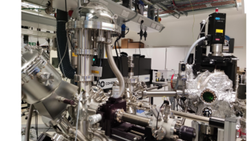
Pulsed laser deposition (PLD)
In PLD, short pulses of a high-energy laser ablate small amounts of a target material by evaporating them into a plasma inside a vacuum chamber. The ablated material is deposited on a substrate opposite to the PLD target. Depending on the deposition conditions such as temperature, partial pressure, or laser energy and frequency, PLD can deposit very pure and uniform epitaxial crystals or completely amorphous thin films. For example, the chamber in the photo was used to deposit ferroelectric thin films of rhombohedral hafnium oxide. PLD is particularly well suited for oxide deposition as a partial oxygen pressure in the evacuated deposition chambers allows for accurate control of the oxygen content of the thin films.
Our systems also have RHEED and XPS capabilities connected to the same vacuum system to allow detailed studies of materials deposition without exposing them to atmosphere.
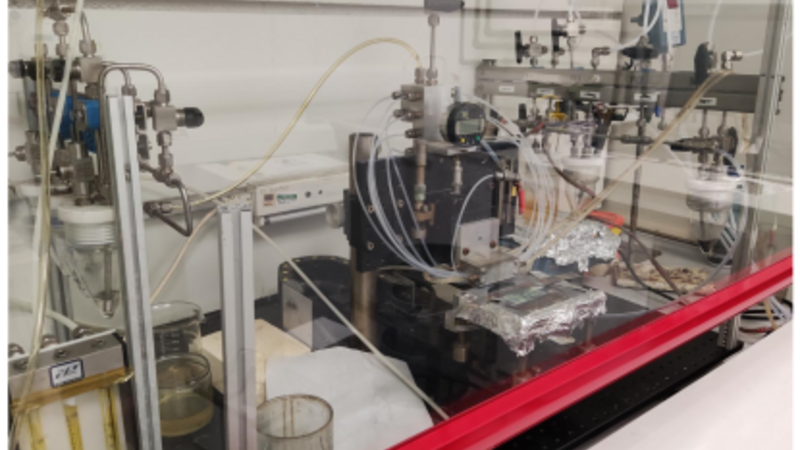
Spatial Atomic Layer Deposition (SALD)
In conventional ALD, the deposition substrate is exposed to the precursor gases sequentially in time, i.e., first to precursor 1, which is then purged from the chamber to make room for precursor 2 afterwards, and so on. In SALD instead, the precursor gases are separated spatially. The precursor gases stream out of the precursor head continuously, but are separated by inert gas outlets between the different precursors. The substrate is then exposed to the precursors by oscillating the precursor head over it and by this movement, the substrate is exposed only to one precursor at a time. While thin films can be deposited with the same quality as in conventional ALD, SALD is a much faster process, because it does not require the purge times of conventional ALD. We have even demonstrated deposition of epitaxial films with this system and the setup has been replicated in several other labs around the world.
Sputter Deposition
We procured a new state of the art AJA sputter deposition system in 2023, which is situated in the Electrical Engineering cleanroom. In a sputter system, in a low-pressure atmosphere, a plasma of a sputter gas like Ar impacts on a target and ejects material from it. The ejected material travels through the low-pressure atmosphere and is deposited on a suitable substrate. This enables the deposition of a large variety of functional thin films from metallic TiN to resistive switching oxides.
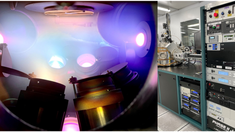
The deposition chamber can achieve a base pressure better than 8×10⁻⁸ Torr and the 4-inch Inconel substrate holder can be heated up to 900 °C (with a uniformity better than ± 1% across the substrate holder). It can be continuously rotated (0-40 rpm) during deposition and is connected to a DC/RF power supply that provides substrate potential. The advanced system is currently equipped with seven 2-inch magnetron sputtering sources, with a possibility to add two more. It has five on-axis sources symmetrically mounted in the bottom of the chamber and two off-axis sources with a 90° angle with respect to the substrate holder. The off-axis sources are perfect for growing epitaxial layers. The angle of all sputtering sources can be controllably changed, which provides a great possibility for glancing-angle magnetron sputtering; growing functional thin films with dense zig-zag tilted-nanostructures. The Driscoll sputtering system is equipped with all power supplies that exist for magnetron sputtering; RF, DC, and bipolar HiPIMS (High Power Impulse Magnetron Sputtering) power generators. Compared with RF and DC, which mainly generate sputter-ejected atoms, the HiPIMS power supply is an advanced generator that produces ionised target atoms, the energies of which can be precisely tuned with applying substrate potential. HiPIMS is excellent for growing functional thin films with metastable phases, tuneable nanostructures, and strain. It is worth mentioning that this system is equipped with a bipolar HiPIMS generator, which in addition to negative high-amplitude pulses, can also generate positive pulses. This is key for growing oxides from metal targets in reactive atmospheres to minimise effectively target poisoning during thin film deposition. Finally, this equipment has an external ion source that can provide a variety of gas ions (H, N, and O). This ion source can be used both during or after growth to provide different possibilities to tune thin films properties.
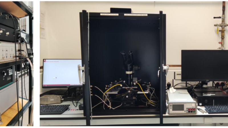
Electrical Measurement Suite
We have several electrical characterisation suites, one of which in the photo below. It comprises a probe station, two ferroelectric testers (Radiant and Aixacct), a versatile source/measure unit (Keysight B2912), and an impedance analyser (Solartron Analytical). The setup is used on a daily basis by many different users for a wide range of applications including standard current-voltage measurements, but also demonstrations of neuromorphic learning capabilities, and battery and fuel cell research.
More content coming soon on, e.g., X-ray diffraction, Atomic Force Microscopy, UV lithography, Transmission Electron Microscopy, ...